- 您现在的位置:买卖IC网 > Sheet目录3881 > PIC18F8585T-I/PT (Microchip Technology)IC PIC MCU FLASH 24KX16 80TQFP
PIC18F6585/8585/6680/8680
DS30491C-page 34
2004 Microchip Technology Inc.
3.1
Power-on Reset (POR)
A Power-on Reset pulse is generated on-chip when
VDD rise is detected. To take advantage of the POR cir-
cuitry, tie the MCLR pin through a 1 k
to 10 k resis-
tor to VDD. This will eliminate external RC components
usually needed to create a Power-on Reset delay. A
minimum rise rate for VDD is specified (parameter
D004). For a slow rise time, see Figure 3-2.
When the device starts normal operation (i.e., exits the
Reset condition), device operating parameters (volt-
age, frequency, temperature, etc.) must be met to
ensure operation. If these conditions are not met, the
device must be held in Reset until the operating
conditions are met.
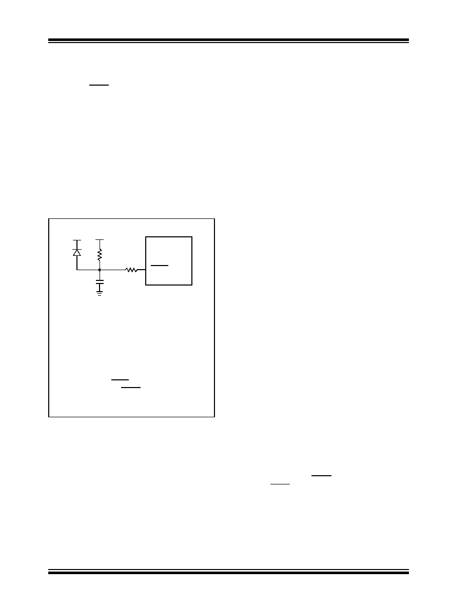
FIGURE 3-2:
EXTERNAL POWER-ON
RESET CIRCUIT (FOR
SLOW VDD POWER-UP)
3.2
Power-up Timer (PWRT)
The Power-up Timer provides a fixed nominal time-out
(parameter #33) only on power-up from the POR. The
Power-up Timer operates on an internal RC oscillator.
The chip is kept in Reset as long as the PWRT is active.
The PWRT’s time delay allows VDD to rise to an
acceptable level. A configuration bit is provided to
enable/disable the PWRT.
The power-up time delay will vary from chip-to-chip due
to VDD, temperature and process variation. See DC
parameter #33 for details.
3.3
Oscillator Start-up Timer (OST)
The Oscillator Start-up Timer (OST) provides 1024
oscillator cycles (from OSC1 input) delay after the
PWRT delay is over (parameter #32). This ensures that
the crystal oscillator or resonator has started and
stabilized.
The OST time-out is invoked only for XT, LP and HS
modes and only on Power-on Reset, or wake-up from
Sleep.
3.4
PLL Lock Time-out
With the PLL enabled, the time-out sequence following
a Power-on Reset is different from other oscillator
modes. A portion of the Power-up Timer is used to pro-
vide a fixed time-out that is sufficient for the PLL to lock
to the main oscillator frequency. This PLL lock time-out
(TPLL) is typically 2 ms and follows the oscillator
start-up time-out (OST).
3.5
Brown-out Reset (BOR)
A configuration bit, BOREN, can disable (if clear/
programmed), or enable (if set) the Brown-out Reset
circuitry. If VDD falls below parameter D005 for greater
than parameter #35, the brown-out situation will reset
the chip. A Reset may not occur if VDD falls below
parameter D005 for less than parameter #35. The chip
will remain in Brown-out Reset until VDD rises above
BVDD. If the Power-up Timer is enabled, it will be
invoked after VDD rises above BVDD; it then will keep
the chip in Reset for an additional time delay (parame-
ter #33). If VDD drops below BVDD while the Power-up
Timer is running, the chip will go back into a Brown-out
Reset and the Power-up Timer will be initialized. Once
VDD rises above BVDD, the Power-up Timer will
execute the additional time delay.
3.6
Time-out Sequence
On power-up, the time-out sequence is as follows:
First, PWRT time-out is invoked after the POR time
delay has expired. Then, OST is activated. The total
time-out will vary based on oscillator configuration and
the status of the PWRT. For example, in RC mode with
the PWRT disabled, there will be no time-out at all.
Figure 3-7 depict time-out sequences on power-up.
Since the time-outs occur from the POR pulse, the
time-outs will expire if MCLR is kept low long enough.
Bringing MCLR high will begin execution immediately
(Figure 3-5). This is useful for testing purposes or to
synchronize more than one PIC18FXX8X device
operating in parallel.
Table 3-2 shows the Reset conditions for some Special
Function Registers while Table 3-3 shows the Reset
conditions for all of the registers.
Note 1:
External Power-on Reset circuit is required
only if the VDD power-up slope is too slow.
The diode D helps discharge the capacitor
quickly when VDD powers down.
2:
R < 40 k
is recommended to make sure that
the voltage drop across R does not violate
the device’s electrical specification.
3:
R1 = 1 k
to 10 k will limit any current flow-
ing into MCLR from external capacitor C, in
the event of MCLR/VPP pin breakdown due to
Electrostatic Discharge (ESD) or Electrical
Overstress (EOS).
C
R1
R
D
VDD
MCLR
PIC18FXX8X
发布紧急采购,3分钟左右您将得到回复。
相关PDF资料
XF2J-2424-11
CONN FPC 24POS 0.5MM SMT
PIC18LF6585T-I/PT
IC PIC MCU FLASH 24KX16 64TQFP
PIC18LF6680T-I/PT
IC PIC MCU FLASH 32KX16 64TQFP
XF2J-2224-11
CONN FPC 22POS 0.5MM SMT
PIC18F6525T-I/PT
IC PIC MCU FLASH 24KX16 64TQFP
PIC18F4439-E/ML
IC PIC MCU FLASH 6KX16 44QFN
XF2J-2024-11
CONN FPC 20POS 0.5MM SMT
PIC16LF747-I/ML
IC PIC MCU FLASH 4KX14 44QFN
相关代理商/技术参数
PIC18F85J10-I/PT
功能描述:8位微控制器 -MCU 32 KB FL 2 KB RAM RoHS:否 制造商:Silicon Labs 核心:8051 处理器系列:C8051F39x 数据总线宽度:8 bit 最大时钟频率:50 MHz 程序存储器大小:16 KB 数据 RAM 大小:1 KB 片上 ADC:Yes 工作电源电压:1.8 V to 3.6 V 工作温度范围:- 40 C to + 105 C 封装 / 箱体:QFN-20 安装风格:SMD/SMT
PIC18F85J10-I/PT
制造商:Microchip Technology Inc 功能描述:IC 8BIT MCU PIC18F 40MHZ TQFP-80 制造商:Microchip Technology Inc 功能描述:IC, 8BIT MCU, PIC18F, 40MHZ, TQFP-80
PIC18F85J10T-I/PT
功能描述:8位微控制器 -MCU 32 KB FL 2 KB RAM RoHS:否 制造商:Silicon Labs 核心:8051 处理器系列:C8051F39x 数据总线宽度:8 bit 最大时钟频率:50 MHz 程序存储器大小:16 KB 数据 RAM 大小:1 KB 片上 ADC:Yes 工作电源电压:1.8 V to 3.6 V 工作温度范围:- 40 C to + 105 C 封装 / 箱体:QFN-20 安装风格:SMD/SMT
PIC18F85J11-I/PT
功能描述:8位微控制器 -MCU 32KB Flash 2048BRAM 67I/O RoHS:否 制造商:Silicon Labs 核心:8051 处理器系列:C8051F39x 数据总线宽度:8 bit 最大时钟频率:50 MHz 程序存储器大小:16 KB 数据 RAM 大小:1 KB 片上 ADC:Yes 工作电源电压:1.8 V to 3.6 V 工作温度范围:- 40 C to + 105 C 封装 / 箱体:QFN-20 安装风格:SMD/SMT
PIC18F85J11T-I/PT
功能描述:8位微控制器 -MCU 32KB Flash 2048bytes-RAM 67I/O RoHS:否 制造商:Silicon Labs 核心:8051 处理器系列:C8051F39x 数据总线宽度:8 bit 最大时钟频率:50 MHz 程序存储器大小:16 KB 数据 RAM 大小:1 KB 片上 ADC:Yes 工作电源电压:1.8 V to 3.6 V 工作温度范围:- 40 C to + 105 C 封装 / 箱体:QFN-20 安装风格:SMD/SMT
PIC18F85J15-I/PT
功能描述:8位微控制器 -MCU 48 KB FL 4 KB RAM RoHS:否 制造商:Silicon Labs 核心:8051 处理器系列:C8051F39x 数据总线宽度:8 bit 最大时钟频率:50 MHz 程序存储器大小:16 KB 数据 RAM 大小:1 KB 片上 ADC:Yes 工作电源电压:1.8 V to 3.6 V 工作温度范围:- 40 C to + 105 C 封装 / 箱体:QFN-20 安装风格:SMD/SMT
PIC18F85J15T-I/PT
功能描述:8位微控制器 -MCU 48 KB FL 4 KB RAM RoHS:否 制造商:Silicon Labs 核心:8051 处理器系列:C8051F39x 数据总线宽度:8 bit 最大时钟频率:50 MHz 程序存储器大小:16 KB 数据 RAM 大小:1 KB 片上 ADC:Yes 工作电源电压:1.8 V to 3.6 V 工作温度范围:- 40 C to + 105 C 封装 / 箱体:QFN-20 安装风格:SMD/SMT
PIC18F85J50-I/PT
功能描述:8位微控制器 -MCU 32KB Flash 3936byte RAM RoHS:否 制造商:Silicon Labs 核心:8051 处理器系列:C8051F39x 数据总线宽度:8 bit 最大时钟频率:50 MHz 程序存储器大小:16 KB 数据 RAM 大小:1 KB 片上 ADC:Yes 工作电源电压:1.8 V to 3.6 V 工作温度范围:- 40 C to + 105 C 封装 / 箱体:QFN-20 安装风格:SMD/SMT